
California CRE News In Your Inbox.
Sign up for Connect emails to stay informed with CRE stories that are 150 words or less.

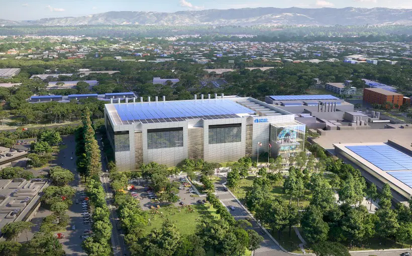

Applied Materials Plans $4B Semiconductor Facility for Silicon Valley
Applied Materials, Inc. said Monday it would build the world’s largest and most advanced facility for collaborative semiconductor process technology and manufacturing equipment research and development. The new Equipment and Process Innovation and Commercialization (EPIC) Center will be built on an Applied Materials campus in Sunnyvale within Silicon Valley, and the company plans to spend upwards of $4 billion on the project.
The new facility will contain more than 180,000 square feet of cleanroom for collaborative innovation with chipmakers, universities and ecosystem partners. It’s expected to reduce the time it takes the industry to bring a technology from concept to commercialization by several years.
“This investment presents a golden opportunity to re-engineer the way the global industry collaborates to deliver the foundational semiconductor process and manufacturing technologies needed to sustain rapid improvements in energy-efficient, high-performance computing,” said Gary Dickerson, president and CEO of Santa Clara, CA-based Applied Materials.
- ◦Development