


National CRE News In Your Inbox.
Sign up for Connect emails to stay informed with CRE stories that are 150 words or less.


The Shift of Global Semiconductor Location Strategies
One mantra of successful commercial real estate operations has boiled down to three words: Location, location, location. This has held, whether the asset in question is a multifamily property, a retail center, or a semiconductor physical fabrication plant—“fab” for short.
According to JLL, the goals of an optimal location once included access to knowledgeable labor, reliable infrastructure and lower operating costs.
That was then. In its recent article, “Remapping the Global Semiconductor Industry,” JLL said that the huge growth of artificial intelligence, combined with concerns over trade issues and supply chain disruptions, means that location strategies are focused on “a more diversified and policy-driven global footprint.”
In other words, the industry is undergoing what JLL analysts called a “Great Rebalancing,” which involves understanding economics, supply chain resilience, and policy intervention.
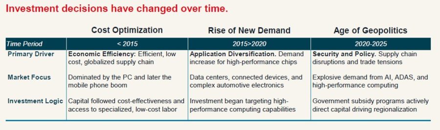
For example, semiconductor manufacturing was concentrated in Taiwan and the Netherlands. These days, “those areas now present resilience challenges, due to geopolitical, environmental or infrastructure concerns,” the JLL write-up said. Additionally, capital investments in fabs can also be determined by public policy and national security priorities.
As a result, other countries and regions have stepped in with offers. The United States is attracting wager fabs. Southeast Asia is benefitting from “China Plus One” strategies, while India continues to grow in its role as a critical R&D hub.
Another factor is that the semiconductor value chain is more fragmented. As a result, “R&D, fabrication, and advanced packaging each have unique needs for talent, utilities, energy reliability, water access, and ecosystem maturity, which means that finding a one-size-fits-all location is impractical,” the article noted.
JLL explained that location strategies should go beyond cost and talent to include the following:
- Considering locations based on the entire semiconductor value chain and understanding talent, utilities and infrastructure needs
- Securing maximum value through multibillion-dollar government incentive packages
- Mitigating geopolitical risk by moving beyond the usual concentrations to build a robust and functional supply chain
- Vetting and researching emerging locations to ensure they offer the necessary talent and infrastructure to support long-term investments
- ◦Development
- ◦Policy/Gov't
